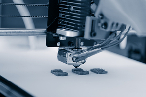
 3D printing in a factory setting, otherwise known as additive manufacturing (AM) is coming of age as a production technique. It brings considerable advantages for electronic manufacturers, particularly for those who need flexibility and customisation in the shape, functionality and composition of the Printed Circuit Boards (PCBs) they use.
“We did it! We made a whistle!”
So says uber-nerd Howard Wolowitz in The Big Bang Theory as he extracts his underwhelming prize from his massively expensive 3D printer after several hours wait. And this has long been the perceived problem with 3D printing as a manufacturing solution - it has been widely regarded as too slow, too expensive and impossible to scale cost-effectively.
Many of these fundamental issues remain for many industries. But, as the range of materials that can be used for fabrication increases and more customisation is required for lower runs of higher value products - AM is being used more and more, as part of the mix of the electronics manufacturing process.
But first, some definitions:
What is Additive Manufacturing?
Additive manufacturing is the process of using computer-aided-design (CAD) software or 3D object scanners to direct 3D printing hardware to deposit material, layer upon layer, in precise geometric shapes as part of a production line process.
When should you use AM?
This checklist from Manufacturing Tomorrow remains a useful guide for those considering additive manufacturing as a solution for the production of parts - and is useful for PCB designers to consider, too:
- Is it a complicated part?
- Is it low volume?
- Is it high value?
- Is development and tooling time considerable?
- Does it require personalisation or customisation?
- If it is many parts could it be made from less?
Why use AM for PCB manufacture?
PCBs have typically been made in a rectangular shape to reduce waste and increase the speed of manufacturing throughput.
But as electronic devices have become smaller and more sophisticated, so the demand for multi-layer boards to fit more compact and uniquely shaped interiors has grown.
In a traditional production line setting, the more complex a board becomes and the higher the layer count, the more time consuming and expensive it becomes to assemble non-standard shapes.
AM supports complex shape and non-planar geometry in PCB design
However, with additive manufacturing individual PCBs and multi-board systems can be printed in complex shapes and even in non-planar geometry (e.g curved or of varying thickness) as required. The layer-by-layer printing process allows components to be embedded or mounted on the side of a non-planar PCB substrate. It also allows unique interconnect architecture to be created, such as horizontal, diagonal, or curved vias.
3D printing allows the production of custom conductive components with unique functionality and geometry. These include conductive sensing elements, certain antennas, inductors or coils, as well as embedded capacitors.
Now a wider range of advanced materials have become available for use in commercial 3D printers, including semiconducting polymers, even more passive and active devices can be printed directly on a surface layer or an interior layer.
Additive manufacturer can improve PCB performance
Additively manufactured PCBs can be designed and manufactured more easily to fit into devices with any form factor. This improves the performance of the components, as well as minimising size and optimising weight, fitting them for use in wearables and other small but powerful IoT technologies.
With more form factor freedom, customisation, and greater support for more novel functionality - additive manufacturing answers many of the most pressing challenges of the electronics manufacturing industry.
As devices miniaturise, become smarter and require more flexibility for use in more challenging conditions, the intricacy and personalisation supported by 3D printing makes sense as a fabrication method.
But it also promises to change supply chain relationships in ways that are potentially more cost-effective and better for the planet.
Additive Manufacturing: An on-demand technology
AM can pave the way for on-demand, just-in-time production which makes processes leaner and more efficient overall.
Additive manufacturing is by its nature digitised and this presents a huge opportunity for PCB designers. With the right integrations and relationships with their production partners, companies will be able to experiment with new designs, as well as replace and order new components in exactly the quantity they need, when they need it. This could mean less waste for everyone, with a supply chain that is much less volatile and unpredictable in terms of cost and availability.
Working out whether AM is the right solution for you will be a function of the required sophistication of your end products and the budgetary constraints you are working under.

