 At the product design stage, original equipment manufacturers (OEMs) must decide how configurable they want their products to be. They usually have two options: control upgrades to the product through software releases or design the product to support additional hardware.
In many electronics-based products the printed circuit board assembly (PCBA) will often be well-hidden, potted or even locked away; helping to protect intellectual property, retain control of software upgrades and minimise the risk of field failures and warranty claims thanks to end users "tinkering". Smartphones are a good example of this. Both Google and Apple tightly control all updates when it comes to their Android and iOS platforms.
However, when an OEM supports hardware upgrades, they must decide the best way of making the connections between the main board and peripheral cards. In this blog post, we will look at some of the benefits of using edge connectors to make these connections.
We will also consider some of the challenges associated with producing the mating printed circuit board (PCB) and why close communication and co-operation between the PCB supplier, connector manufacturer and whoever is manufacturing the product - be it the OEM themselves or their chosen electronics manufacturing services (EMS) partner is vital.
What are edge connectors?
An edge connector consists of a female connector designed to mate with exposed contact pads along the edge of a printed circuit board. Edge connectors are often used as a way of saving space when "real estate" on the main board is limited. They offer a robust connection and are simple to use as they allow mating cards to slot easily in and out.
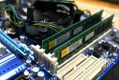
One of the big benefits of using them is that they help to reduce cost. A male connector is not required on the mating card - therefore, removing both the material cost and the assembly time to fit it. A common use of edge connectors is within personal computers; the motherboard has a range of edge connectors built in to allow additional memory or graphics cards to be fitted or replaced.
The mating half
When designing the PCB to mate with edge connectors, there are a number of things to consider. The first is to verify the information supplied by the interconnect manufacturer. Specifically, check that the chamfer angle and tolerances needed for the mating edge suit your design and the capabilities of your PCB supplier.
Many interconnect manufacturers will provide PCB, stencil and mating card layout information for OEMs to use as a reference. It’s worth double checking though how close to these recommendations you need to work to.
Bear in mind the connector manufacturer could be producing millions of the same part across a broad customer base. So while the data should be accurate, they clearly won’t be familiar with your design and application, nor will they have an appreciation of your PCB supplier's equipment and processes.
Communicate closely and document changes
As a result, you may find the connector manufacturer advises working closely with the circuit board manufacturer to arrive at an achievable design, as close to the original recommendations as possible. It will still be important to build in some degree of chamfer, to serve as a lead-in to the connector contact area without causing damage. But you may find the chamfer angle and tolerance differs to the original datasheet.
Once you are comfortable that the chamfer angle and tolerances suit the mating PCB and can be consistently produced by the circuit board supplier, document any changes to the original datasheet. This information should be contained within the Gerber file but, to ensure that it does not get missed or interpreted incorrectly, it’s recommended a separate drawing is created showing the dimensions.
This is particularly important if you are considering outsourcing the manufacturing of the PCBA at any stage to an EMS provider, or there is any possibility that your PCB manufacturer could change over time.
Challenges faced by PCB suppliers and electronics manufacturers
Applying a bevel or chamfer to the mating PCB requires specialist equipment and tight process control. Some PCB suppliers will be more familiar with this process than others. It’s important to make sure that the PCB supplier you intend to work with understands your instructions and can provide boards in the production quantities you require.
If the process is not standard for them, then you may find that they will need to invest in additional equipment or sub contract this element of the process out – all of which could increase the cost of the bare board.
On receipt of bare boards, it can be difficult for OEMs or EMS providers to measure accurately the chamfer angle and tolerance, due to the PCB tooling border obscuring the view. As a result, discrepancies may not always get picked up until the tooling border has been removed or the physical mating cycle takes place with the female connector.
To overcome this issue you could request that the PCB supplier chamfers the tooling border as well, effectively mirroring the angle applied to the circuit board. Alternatively, part of the tooling border could be removed from the connector edge of the PCB prior to assembly but this would need discussing with the production team responsible for populating the board in case this causes them any other issues.
So there you have it - the benefits of using edge connectors along with some of the challenges associated with producing the PCBs that mate with them. As ever, a robust new product introduction (NPI) process should be followed to ensure any issues are identified and resolved before entering into volume build, to avoid ending up with piles of scrap boards.
Image by machu

